
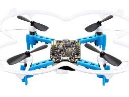
正点原子MiniFly Firmware V1.5开源四轴代码分析三:时钟配置system_stm32f4xx.c。
正点原子MiniFly Firmware V1.5开源四轴代码分析三:时钟配置system_stm32f4xx.c。
·
cc
/**
******************************************************************************
* @file system_stm32f4xx.c
* @author MCD Application Team
* @version V1.4.0
* @date 04-August-2014
* @brief CMSIS Cortex-M4 Device Peripheral Access Layer System Source File.
* This file contains the system clock configuration for STM32F4xx devices.
*
* 1. This file provides two functions and one global variable to be called from
* user application:
* - SystemInit(): Setups the system clock (System clock source, PLL Multiplier
* and Divider factors, AHB/APBx prescalers and Flash settings),
* depending on the configuration made in the clock xls tool.
* This function is called at startup just after reset and
* before branch to main program. This call is made inside
* the "startup_stm32f4xx.s" file.
*
* - SystemCoreClock variable: Contains the core clock (HCLK), it can be used
* by the user application to setup the SysTick
* timer or configure other parameters.
*
* - SystemCoreClockUpdate(): Updates the variable SystemCoreClock and must
* be called whenever the core clock is changed
* during program execution.
*
* 2. After each device reset the HSI (16 MHz) is used as system clock source.
* Then SystemInit() function is called, in "startup_stm32f4xx.s" file, to
* configure the system clock before to branch to main program.
*
* 3. If the system clock source selected by user fails to startup, the SystemInit()
* function will do nothing and HSI still used as system clock source. User can
* add some code to deal with this issue inside the SetSysClock() function.
*
* 4. The default value of HSE crystal is set to 25MHz, refer to "HSE_VALUE" define
* in "stm32f4xx.h" file. When HSE is used as system clock source, directly or
* through PLL, and you are using different crystal you have to adapt the HSE
* value to your own configuration.
*
* 5. This file configures the system clock as follows:
*=============================================================================
*=============================================================================
* Supported STM32F40xxx/41xxx devices
*-----------------------------------------------------------------------------
* System Clock source | PLL (HSE)
*-----------------------------------------------------------------------------
* SYSCLK(Hz) | 168000000
*-----------------------------------------------------------------------------
* HCLK(Hz) | 168000000
*-----------------------------------------------------------------------------
* AHB Prescaler | 1
*-----------------------------------------------------------------------------
* APB1 Prescaler | 4
*-----------------------------------------------------------------------------
* APB2 Prescaler | 2
*-----------------------------------------------------------------------------
* HSE Frequency(Hz) | 25000000
*-----------------------------------------------------------------------------
* PLL_M | 25
*-----------------------------------------------------------------------------
* PLL_N | 336
*-----------------------------------------------------------------------------
* PLL_P | 2
*-----------------------------------------------------------------------------
* PLL_Q | 7
*-----------------------------------------------------------------------------
* PLLI2S_N | NA
*-----------------------------------------------------------------------------
* PLLI2S_R | NA
*-----------------------------------------------------------------------------
* I2S input clock | NA
*-----------------------------------------------------------------------------
* VDD(V) | 3.3
*-----------------------------------------------------------------------------
* Main regulator output voltage | Scale1 mode
*-----------------------------------------------------------------------------
* Flash Latency(WS) | 5
*-----------------------------------------------------------------------------
* Prefetch Buffer | ON
*-----------------------------------------------------------------------------
* Instruction cache | ON
*-----------------------------------------------------------------------------
* Data cache | ON
*-----------------------------------------------------------------------------
* Require 48MHz for USB OTG FS, | Disabled
* SDIO and RNG clock |
*-----------------------------------------------------------------------------
*=============================================================================
*=============================================================================
* Supported STM32F42xxx/43xxx devices
*-----------------------------------------------------------------------------
* System Clock source | PLL (HSE)
*-----------------------------------------------------------------------------
* SYSCLK(Hz) | 180000000
*-----------------------------------------------------------------------------
* HCLK(Hz) | 180000000
*-----------------------------------------------------------------------------
* AHB Prescaler | 1
*-----------------------------------------------------------------------------
* APB1 Prescaler | 4
*-----------------------------------------------------------------------------
* APB2 Prescaler | 2
*-----------------------------------------------------------------------------
* HSE Frequency(Hz) | 25000000
*-----------------------------------------------------------------------------
* PLL_M | 25
*-----------------------------------------------------------------------------
* PLL_N | 360
*-----------------------------------------------------------------------------
* PLL_P | 2
*-----------------------------------------------------------------------------
* PLL_Q | 7
*-----------------------------------------------------------------------------
* PLLI2S_N | NA
*-----------------------------------------------------------------------------
* PLLI2S_R | NA
*-----------------------------------------------------------------------------
* I2S input clock | NA
*-----------------------------------------------------------------------------
* VDD(V) | 3.3
*-----------------------------------------------------------------------------
* Main regulator output voltage | Scale1 mode
*-----------------------------------------------------------------------------
* Flash Latency(WS) | 5
*-----------------------------------------------------------------------------
* Prefetch Buffer | ON
*-----------------------------------------------------------------------------
* Instruction cache | ON
*-----------------------------------------------------------------------------
* Data cache | ON
*-----------------------------------------------------------------------------
* Require 48MHz for USB OTG FS, | Disabled
* SDIO and RNG clock |
*-----------------------------------------------------------------------------
*=============================================================================
*=============================================================================
* Supported STM32F401xx devices
*-----------------------------------------------------------------------------
* System Clock source | PLL (HSE)
*-----------------------------------------------------------------------------
* SYSCLK(Hz) | 84000000
*-----------------------------------------------------------------------------
* HCLK(Hz) | 84000000
*-----------------------------------------------------------------------------
* AHB Prescaler | 1
*-----------------------------------------------------------------------------
* APB1 Prescaler | 2
*-----------------------------------------------------------------------------
* APB2 Prescaler | 1
*-----------------------------------------------------------------------------
* HSE Frequency(Hz) | 25000000
*-----------------------------------------------------------------------------
* PLL_M | 25
*-----------------------------------------------------------------------------
* PLL_N | 336
*-----------------------------------------------------------------------------
* PLL_P | 4
*-----------------------------------------------------------------------------
* PLL_Q | 7
*-----------------------------------------------------------------------------
* PLLI2S_N | NA
*-----------------------------------------------------------------------------
* PLLI2S_R | NA
*-----------------------------------------------------------------------------
* I2S input clock | NA
*-----------------------------------------------------------------------------
* VDD(V) | 3.3
*-----------------------------------------------------------------------------
* Main regulator output voltage | Scale1 mode
*-----------------------------------------------------------------------------
* Flash Latency(WS) | 2
*-----------------------------------------------------------------------------
* Prefetch Buffer | ON
*-----------------------------------------------------------------------------
* Instruction cache | ON
*-----------------------------------------------------------------------------
* Data cache | ON
*-----------------------------------------------------------------------------
* Require 48MHz for USB OTG FS, | Disabled
* SDIO and RNG clock |
*-----------------------------------------------------------------------------
*=============================================================================
*=============================================================================
* Supported STM32F411xx devices
*-----------------------------------------------------------------------------
* System Clock source | PLL (HSI)
*-----------------------------------------------------------------------------
* SYSCLK(Hz) | 100000000
*-----------------------------------------------------------------------------
* HCLK(Hz) | 100000000
*-----------------------------------------------------------------------------
* AHB Prescaler | 1
*-----------------------------------------------------------------------------
* APB1 Prescaler | 2
*-----------------------------------------------------------------------------
* APB2 Prescaler | 1
*-----------------------------------------------------------------------------
* HSI Frequency(Hz) | 16000000
*-----------------------------------------------------------------------------
* PLL_M | 16
*-----------------------------------------------------------------------------
* PLL_N | 400
*-----------------------------------------------------------------------------
* PLL_P | 4
*-----------------------------------------------------------------------------
* PLL_Q | 7
*-----------------------------------------------------------------------------
* PLLI2S_N | NA
*-----------------------------------------------------------------------------
* PLLI2S_R | NA
*-----------------------------------------------------------------------------
* I2S input clock | NA
*-----------------------------------------------------------------------------
* VDD(V) | 3.3
*-----------------------------------------------------------------------------
* Main regulator output voltage | Scale1 mode
*-----------------------------------------------------------------------------
* Flash Latency(WS) | 3
*-----------------------------------------------------------------------------
* Prefetch Buffer | ON
*-----------------------------------------------------------------------------
* Instruction cache | ON
*-----------------------------------------------------------------------------
* Data cache | ON
*-----------------------------------------------------------------------------
* Require 48MHz for USB OTG FS, | Disabled
* SDIO and RNG clock |
*-----------------------------------------------------------------------------
*=============================================================================
******************************************************************************
* @attention
*
* <h2><center>© COPYRIGHT 2014 STMicroelectronics</center></h2>
*
* Licensed under MCD-ST Liberty SW License Agreement V2, (the "License");
* You may not use this file except in compliance with the License.
* You may obtain a copy of the License at:
*
* http://www.st.com/software_license_agreement_liberty_v2
*
* Unless required by applicable law or agreed to in writing, software
* distributed under the License is distributed on an "AS IS" BASIS,
* WITHOUT WARRANTIES OR CONDITIONS OF ANY KIND, either express or implied.
* See the License for the specific language governing permissions and
* limitations under the License.
*
******************************************************************************
*/
/** @addtogroup CMSIS
* @{
*/
/** @addtogroup stm32f4xx_system
* @{
*/
/** @addtogroup STM32F4xx_System_Private_Includes
* @{
*/
#include "stm32f4xx.h"
/**
* @}
*/
/** @addtogroup STM32F4xx_System_Private_TypesDefinitions
* @{
*/
/**
* @}
*/
/** @addtogroup STM32F4xx_System_Private_Defines
* @{
*/
/************************* Miscellaneous Configuration ************************/
/*!< Uncomment the following line if you need to use external SRAM or SDRAM mounted
on STM324xG_EVAL/STM324x7I_EVAL/STM324x9I_EVAL boards as data memory */
#if defined (STM32F40_41xxx) || defined (STM32F427_437xx) || defined (STM32F429_439xx)
/* #define DATA_IN_ExtSRAM */
#endif /* STM32F40_41xxx || STM32F427_437x || STM32F429_439xx */
#if defined (STM32F427_437xx) || defined (STM32F429_439xx)
/* #define DATA_IN_ExtSDRAM */
#endif /* STM32F427_437x || STM32F429_439xx */
#if defined (STM32F411xE)
/*!< Uncomment the following line if you need to clock the STM32F411xE by HSE Bypass
through STLINK MCO pin of STM32F103 microcontroller. The frequency cannot be changed
and is fixed at 8 MHz.
Hardware configuration needed for Nucleo Board:
?SB54, SB55 OFF
?R35 removed
?SB16, SB50 ON */
#define USE_HSE_BYPASS
#if defined (USE_HSE_BYPASS)
#define HSE_BYPASS_INPUT_FREQUENCY 8000000
#endif /* USE_HSE_BYPASS */
#endif /* STM32F411xE */
/*!< Uncomment the following line if you need to relocate your vector Table in
Internal SRAM. */
/* #define VECT_TAB_SRAM */
#define VECT_TAB_OFFSET 0x0 /*!< Vector Table base offset field.
This value must be a multiple of 0x200. */
/******************************************************************************/
/************************* PLL Parameters *************************************/
#if defined (STM32F40_41xxx) || defined (STM32F427_437xx) || defined (STM32F429_439xx) || defined (STM32F401xx)
/* PLL_VCO = (HSE_VALUE or HSI_VALUE / PLL_M) * PLL_N */
#define PLL_M 8
#else /* STM32F411xE */
#if defined (USE_HSE_BYPASS)
#define PLL_M 8
#else /* STM32F411xE */
#define PLL_M 16
#endif /* USE_HSE_BYPASS */
#endif /* STM32F40_41xxx || STM32F427_437xx || STM32F429_439xx || STM32F401xx */
/* USB OTG FS, SDIO and RNG Clock = PLL_VCO / PLLQ */
#define PLL_Q 4 /* USB OTG FS=192/4=48MHz */
#if defined (STM32F40_41xxx)
#define PLL_N 336
/* SYSCLK = PLL_VCO / PLL_P */
#define PLL_P 2
#endif /* STM32F40_41xxx */
#if defined (STM32F427_437xx) || defined (STM32F429_439xx)
#define PLL_N 360
/* SYSCLK = PLL_VCO / PLL_P */
#define PLL_P 2
#endif /* STM32F427_437x || STM32F429_439xx */
#if defined (STM32F401xx)
#define PLL_N 336
/* SYSCLK = PLL_VCO / PLL_P */
#define PLL_P 4
#endif /* STM32F401xx */
#if defined (STM32F411xE)
#define PLL_N 192 /* 96*2 50 ≤PLLN ≤432 */
/* SYSCLK = PLL_VCO / PLL_P */
#define PLL_P 2 /* PLLP = 2, 4, 6, or 8 */
#endif /* STM32F411xx */
/******************************************************************************/
/**
* @}
*/
/** @addtogroup STM32F4xx_System_Private_Macros
* @{
*/
/**
* @}
*/
/** @addtogroup STM32F4xx_System_Private_Variables
* @{
*/
#if defined (STM32F40_41xxx)
uint32_t SystemCoreClock = 168000000;
#endif /* STM32F40_41xxx */
#if defined (STM32F427_437xx) || defined (STM32F429_439xx)
uint32_t SystemCoreClock = 180000000;
#endif /* STM32F427_437x || STM32F429_439xx */
#if defined (STM32F401xx)
uint32_t SystemCoreClock = 84000000;
#endif /* STM32F401xx */
#if defined (STM32F411xE)
uint32_t SystemCoreClock = 96000000;
#endif /* STM32F401xx */
__I uint8_t AHBPrescTable[16] = {0, 0, 0, 0, 0, 0, 0, 0, 1, 2, 3, 4, 6, 7, 8, 9};
/**
* @}
*/
/** @addtogroup STM32F4xx_System_Private_FunctionPrototypes
* @{
*/
static void SetSysClock(void);
#if defined (DATA_IN_ExtSRAM) || defined (DATA_IN_ExtSDRAM)
static void SystemInit_ExtMemCtl(void);
#endif /* DATA_IN_ExtSRAM || DATA_IN_ExtSDRAM */
/**
* @}
*/
/** @addtogroup STM32F4xx_System_Private_Functions
* @{
*/
/**
* @brief Setup the microcontroller system
* Initialize the Embedded Flash Interface, the PLL and update the
* SystemFrequency variable.
* @param None
* @retval None
*/
void SystemInit(void)
{
/* FPU settings ------------------------------------------------------------*/
#if (__FPU_PRESENT == 1) && (__FPU_USED == 1)
SCB->CPACR |= ((3UL << 10*2)|(3UL << 11*2)); /* set CP10 and CP11 Full Access */
#endif
/* Reset the RCC clock configuration to the default reset state ------------*/
/* Set HSION bit */
RCC->CR |= (uint32_t)0x00000001;
/* Reset CFGR register */
RCC->CFGR = 0x00000000;
/* Reset HSEON, CSSON and PLLON bits */
RCC->CR &= (uint32_t)0xFEF6FFFF;
/* Reset PLLCFGR register */
RCC->PLLCFGR = 0x24003010;
/* Reset HSEBYP bit */
RCC->CR &= (uint32_t)0xFFFBFFFF;
/* Disable all interrupts */
RCC->CIR = 0x00000000;
#if defined (DATA_IN_ExtSRAM) || defined (DATA_IN_ExtSDRAM)
SystemInit_ExtMemCtl();
#endif /* DATA_IN_ExtSRAM || DATA_IN_ExtSDRAM */
/* Configure the System clock source, PLL Multiplier and Divider factors,
AHB/APBx prescalers and Flash settings ----------------------------------*/
SetSysClock();
/* Configure the Vector Table location add offset address ------------------*/
#ifdef VECT_TAB_SRAM
SCB->VTOR = SRAM_BASE | VECT_TAB_OFFSET; /* Vector Table Relocation in Internal SRAM */
#else
SCB->VTOR = FLASH_BASE | VECT_TAB_OFFSET; /* Vector Table Relocation in Internal FLASH */
#endif
}
/**
* @brief Update SystemCoreClock variable according to Clock Register Values.
* The SystemCoreClock variable contains the core clock (HCLK), it can
* be used by the user application to setup the SysTick timer or configure
* other parameters.
*
* @note Each time the core clock (HCLK) changes, this function must be called
* to update SystemCoreClock variable value. Otherwise, any configuration
* based on this variable will be incorrect.
*
* @note - The system frequency computed by this function is not the real
* frequency in the chip. It is calculated based on the predefined
* constant and the selected clock source:
*
* - If SYSCLK source is HSI, SystemCoreClock will contain the HSI_VALUE(*)
*
* - If SYSCLK source is HSE, SystemCoreClock will contain the HSE_VALUE(**)
*
* - If SYSCLK source is PLL, SystemCoreClock will contain the HSE_VALUE(**)
* or HSI_VALUE(*) multiplied/divided by the PLL factors.
*
* (*) HSI_VALUE is a constant defined in stm32f4xx.h file (default value
* 16 MHz) but the real value may vary depending on the variations
* in voltage and temperature.
*
* (**) HSE_VALUE is a constant defined in stm32f4xx.h file (default value
* 25 MHz), user has to ensure that HSE_VALUE is same as the real
* frequency of the crystal used. Otherwise, this function may
* have wrong result.
*
* - The result of this function could be not correct when using fractional
* value for HSE crystal.
*
* @param None
* @retval None
*/
void SystemCoreClockUpdate(void)
{
uint32_t tmp = 0, pllvco = 0, pllp = 2, pllsource = 0, pllm = 2;
/* Get SYSCLK source -------------------------------------------------------*/
tmp = RCC->CFGR & RCC_CFGR_SWS;
switch (tmp)
{
case 0x00: /* HSI used as system clock source */
SystemCoreClock = HSI_VALUE;
break;
case 0x04: /* HSE used as system clock source */
SystemCoreClock = HSE_VALUE;
break;
case 0x08: /* PLL used as system clock source */
/* PLL_VCO = (HSE_VALUE or HSI_VALUE / PLL_M) * PLL_N
SYSCLK = PLL_VCO / PLL_P
*/
pllsource = (RCC->PLLCFGR & RCC_PLLCFGR_PLLSRC) >> 22;
pllm = RCC->PLLCFGR & RCC_PLLCFGR_PLLM;
#if defined (STM32F40_41xxx) || defined (STM32F427_437xx) || defined (STM32F429_439xx) || defined (STM32F401xx)
if (pllsource != 0)
{
/* HSE used as PLL clock source */
pllvco = (HSE_VALUE / pllm) * ((RCC->PLLCFGR & RCC_PLLCFGR_PLLN) >> 6);
}
else
{
/* HSI used as PLL clock source */
pllvco = (HSI_VALUE / pllm) * ((RCC->PLLCFGR & RCC_PLLCFGR_PLLN) >> 6);
}
#elif defined (STM32F411xE)
#if defined (USE_HSE_BYPASS)
if (pllsource != 0)
{
/* HSE used as PLL clock source */
pllvco = (HSE_BYPASS_INPUT_FREQUENCY / pllm) * ((RCC->PLLCFGR & RCC_PLLCFGR_PLLN) >> 6);
}
#else
if (pllsource == 0)
{
/* HSI used as PLL clock source */
pllvco = (HSI_VALUE / pllm) * ((RCC->PLLCFGR & RCC_PLLCFGR_PLLN) >> 6);
}
#endif /* USE_HSE_BYPASS */
#endif /* STM32F40_41xxx || STM32F427_437xx || STM32F429_439xx || STM32F401xx */
pllp = (((RCC->PLLCFGR & RCC_PLLCFGR_PLLP) >>16) + 1 ) *2;
SystemCoreClock = pllvco/pllp;
break;
default:
SystemCoreClock = HSI_VALUE;
break;
}
/* Compute HCLK frequency --------------------------------------------------*/
/* Get HCLK prescaler */
tmp = AHBPrescTable[((RCC->CFGR & RCC_CFGR_HPRE) >> 4)];
/* HCLK frequency */
SystemCoreClock >>= tmp;
}
/**
* @brief Configures the System clock source, PLL Multiplier and Divider factors,
* AHB/APBx prescalers and Flash settings
* @Note This function should be called only once the RCC clock configuration
* is reset to the default reset state (done in SystemInit() function).
* @param None
* @retval None
*/
static void SetSysClock(void)
{
#if defined (STM32F40_41xxx) || defined (STM32F427_437xx) || defined (STM32F429_439xx) || defined (STM32F401xx)
/******************************************************************************/
/* PLL (clocked by HSE) used as System clock source */
/******************************************************************************/
__IO uint32_t StartUpCounter = 0, HSEStatus = 0;
/* Enable HSE *//外部高速时钟使能
RCC->CR |= ((uint32_t)RCC_CR_HSEON);
/* Wait till HSE is ready and if Time out is reached exit,外部时钟准备好或者超时则退出 */
do
{
HSEStatus = RCC->CR & RCC_CR_HSERDY;
StartUpCounter++;
} while((HSEStatus == 0) && (StartUpCounter != HSE_STARTUP_TIMEOUT));
if ((RCC->CR & RCC_CR_HSERDY) != RESET)//如果外部时钟准备就绪
{
HSEStatus = (uint32_t)0x01; //标志状态为1
}
else
{
HSEStatus = (uint32_t)0x00;
}
if (HSEStatus == (uint32_t)0x01)
{
/* Select regulator voltage output Scale 1 mode */
RCC->APB1ENR |= RCC_APB1ENR_PWREN; //电源接口时钟开启
PWR->CR |= PWR_CR_VOS; //调压器输出电压级别选择 ,1;级别1模式
/* HCLK = SYSCLK / 1*/
RCC->CFGR |= RCC_CFGR_HPRE_DIV1; //AHB不分频
#if defined (STM32F40_41xxx) || defined (STM32F427_437xx) || defined (STM32F429_439xx)
/* PCLK2 = HCLK / 2*/
RCC->CFGR |= RCC_CFGR_PPRE2_DIV2;//AHB2,2分频
/* PCLK1 = HCLK / 4*/
RCC->CFGR |= RCC_CFGR_PPRE1_DIV4; //APB1,4分频
#endif /* STM32F40_41xxx || STM32F427_437x || STM32F429_439xx */
#if defined (STM32F401xx)
/* PCLK2 = HCLK / 2*/
RCC->CFGR |= RCC_CFGR_PPRE2_DIV1;
/* PCLK1 = HCLK / 4*/
RCC->CFGR |= RCC_CFGR_PPRE1_DIV2;
#endif /* STM32F401xx */
/* Configure the main PLL */
RCC->PLLCFGR = PLL_M | (PLL_N << 6) | (((PLL_P >> 1) -1) << 16) |
(RCC_PLLCFGR_PLLSRC_HSE) | (PLL_Q << 24);
/* Enable the main PLL */
RCC->CR |= RCC_CR_PLLON;
/* Wait till the main PLL is ready */
while((RCC->CR & RCC_CR_PLLRDY) == 0)
{
}
#if defined (STM32F427_437xx) || defined (STM32F429_439xx)
/* Enable the Over-drive to extend the clock frequency to 180 Mhz */
PWR->CR |= PWR_CR_ODEN;
while((PWR->CSR & PWR_CSR_ODRDY) == 0)
{
}
PWR->CR |= PWR_CR_ODSWEN;
while((PWR->CSR & PWR_CSR_ODSWRDY) == 0)
{
}
/* Configure Flash prefetch, Instruction cache, Data cache and wait state */
FLASH->ACR = FLASH_ACR_PRFTEN | FLASH_ACR_ICEN |FLASH_ACR_DCEN |FLASH_ACR_LATENCY_5WS;
#endif /* STM32F427_437x || STM32F429_439xx */
#if defined (STM32F40_41xxx)
/* Configure Flash prefetch, Instruction cache, Data cache and wait state */
FLASH->ACR = FLASH_ACR_PRFTEN | FLASH_ACR_ICEN |FLASH_ACR_DCEN |FLASH_ACR_LATENCY_5WS;
#endif /* STM32F40_41xxx */
#if defined (STM32F401xx)
/* Configure Flash prefetch, Instruction cache, Data cache and wait state */
FLASH->ACR = FLASH_ACR_PRFTEN | FLASH_ACR_ICEN |FLASH_ACR_DCEN |FLASH_ACR_LATENCY_2WS;
#endif /* STM32F401xx */
/* Select the main PLL as system clock source */
RCC->CFGR &= (uint32_t)((uint32_t)~(RCC_CFGR_SW));
RCC->CFGR |= RCC_CFGR_SW_PLL;
/* Wait till the main PLL is used as system clock source */
while ((RCC->CFGR & (uint32_t)RCC_CFGR_SWS ) != RCC_CFGR_SWS_PLL);
{
}
}
else
{ /* If HSE fails to start-up, the application will have wrong clock
configuration. User can add here some code to deal with this error */
}
#elif defined (STM32F411xE)
#if defined (USE_HSE_BYPASS)
/******************************************************************************/
/* PLL (clocked by HSE) used as System clock source */
/******************************************************************************/
__IO uint32_t StartUpCounter = 0, HSEStatus = 0;
// /* Enable HSE and HSE BYPASS */
// RCC->CR |= ((uint32_t)RCC_CR_HSEON | RCC_CR_HSEBYP);
/* Enable HSE */
RCC->CR |= ((uint32_t)RCC_CR_HSEON);
/* Wait till HSE is ready and if Time out is reached exit */
do
{
HSEStatus = RCC->CR & RCC_CR_HSERDY;
StartUpCounter++;
} while((HSEStatus == 0) && (StartUpCounter != HSE_STARTUP_TIMEOUT));
if ((RCC->CR & RCC_CR_HSERDY) != RESET)
{
HSEStatus = (uint32_t)0x01;
}
else
{
HSEStatus = (uint32_t)0x00;
}
if (HSEStatus == (uint32_t)0x01)
{
/* Select regulator voltage output Scale 1 mode */
RCC->APB1ENR |= RCC_APB1ENR_PWREN;
PWR->CR |= PWR_CR_VOS;
/* HCLK = SYSCLK / 1*/
RCC->CFGR |= RCC_CFGR_HPRE_DIV1;
/* PCLK2 = HCLK / 1*/
RCC->CFGR |= RCC_CFGR_PPRE2_DIV1;
/* PCLK1 = HCLK / 2*/
RCC->CFGR |= RCC_CFGR_PPRE1_DIV2;
/* Configure the main PLL */
RCC->PLLCFGR = PLL_M | (PLL_N << 6) | (((PLL_P >> 1) -1) << 16) | //PLL_N :192 PLL_P:2 PLL_M=8
(RCC_PLLCFGR_PLLSRC_HSE) | (PLL_Q << 24); //
/* Enable the main PLL */
RCC->CR |= RCC_CR_PLLON;
/* Wait till the main PLL is ready */
while((RCC->CR & RCC_CR_PLLRDY) == 0)
{
}
/* Configure Flash prefetch, Instruction cache, Data cache and wait state */
FLASH->ACR = FLASH_ACR_PRFTEN | FLASH_ACR_ICEN |FLASH_ACR_DCEN |FLASH_ACR_LATENCY_2WS;
/* Select the main PLL as system clock source */
RCC->CFGR &= (uint32_t)((uint32_t)~(RCC_CFGR_SW));
RCC->CFGR |= RCC_CFGR_SW_PLL;
/* Wait till the main PLL is used as system clock source */
while ((RCC->CFGR & (uint32_t)RCC_CFGR_SWS ) != RCC_CFGR_SWS_PLL);
{
}
}
else
{ /* If HSE fails to start-up, the application will have wrong clock
configuration. User can add here some code to deal with this error */
}
#else /* HSI will be used as PLL clock source */
/* Select regulator voltage output Scale 1 mode */
RCC->APB1ENR |= RCC_APB1ENR_PWREN;
PWR->CR |= PWR_CR_VOS;
/* HCLK = SYSCLK / 1*/
RCC->CFGR |= RCC_CFGR_HPRE_DIV1;
/* PCLK2 = HCLK / 2*/
RCC->CFGR |= RCC_CFGR_PPRE2_DIV1;
/* PCLK1 = HCLK / 4*/
RCC->CFGR |= RCC_CFGR_PPRE1_DIV2;
/* Configure the main PLL */
RCC->PLLCFGR = PLL_M | (PLL_N << 6) | (((PLL_P >> 1) -1) << 16) | (PLL_Q << 24);
/* Enable the main PLL */
RCC->CR |= RCC_CR_PLLON;
/* Wait till the main PLL is ready */
while((RCC->CR & RCC_CR_PLLRDY) == 0)
{
}
/* Configure Flash prefetch, Instruction cache, Data cache and wait state */
FLASH->ACR = FLASH_ACR_PRFTEN | FLASH_ACR_ICEN |FLASH_ACR_DCEN |FLASH_ACR_LATENCY_2WS;
/* Select the main PLL as system clock source */
RCC->CFGR &= (uint32_t)((uint32_t)~(RCC_CFGR_SW));
RCC->CFGR |= RCC_CFGR_SW_PLL;
/* Wait till the main PLL is used as system clock source */
while ((RCC->CFGR & (uint32_t)RCC_CFGR_SWS ) != RCC_CFGR_SWS_PLL);
{
}
#endif /* USE_HSE_BYPASS */
#endif /* STM32F40_41xxx || STM32F427_437xx || STM32F429_439xx || STM32F401xx */
}
/**
* @brief Setup the external memory controller. Called in startup_stm32f4xx.s
* before jump to __main
* @param None
* @retval None
*/
#ifdef DATA_IN_ExtSRAM
/**
* @brief Setup the external memory controller.
* Called in startup_stm32f4xx.s before jump to main.
* This function configures the external SRAM mounted on STM324xG_EVAL/STM324x7I boards
* This SRAM will be used as program data memory (including heap and stack).
* @param None
* @retval None
*/
void SystemInit_ExtMemCtl(void)
{
/*-- GPIOs Configuration -----------------------------------------------------*/
/*
+-------------------+--------------------+------------------+--------------+
+ SRAM pins assignment +
+-------------------+--------------------+------------------+--------------+
| PD0 <-> FMC_D2 | PE0 <-> FMC_NBL0 | PF0 <-> FMC_A0 | PG0 <-> FMC_A10 |
| PD1 <-> FMC_D3 | PE1 <-> FMC_NBL1 | PF1 <-> FMC_A1 | PG1 <-> FMC_A11 |
| PD4 <-> FMC_NOE | PE3 <-> FMC_A19 | PF2 <-> FMC_A2 | PG2 <-> FMC_A12 |
| PD5 <-> FMC_NWE | PE4 <-> FMC_A20 | PF3 <-> FMC_A3 | PG3 <-> FMC_A13 |
| PD8 <-> FMC_D13 | PE7 <-> FMC_D4 | PF4 <-> FMC_A4 | PG4 <-> FMC_A14 |
| PD9 <-> FMC_D14 | PE8 <-> FMC_D5 | PF5 <-> FMC_A5 | PG5 <-> FMC_A15 |
| PD10 <-> FMC_D15 | PE9 <-> FMC_D6 | PF12 <-> FMC_A6 | PG9 <-> FMC_NE2 |
| PD11 <-> FMC_A16 | PE10 <-> FMC_D7 | PF13 <-> FMC_A7 |-----------------+
| PD12 <-> FMC_A17 | PE11 <-> FMC_D8 | PF14 <-> FMC_A8 |
| PD13 <-> FMC_A18 | PE12 <-> FMC_D9 | PF15 <-> FMC_A9 |
| PD14 <-> FMC_D0 | PE13 <-> FMC_D10 |-----------------+
| PD15 <-> FMC_D1 | PE14 <-> FMC_D11 |
| | PE15 <-> FMC_D12 |
+------------------+------------------+
*/
/* Enable GPIOD, GPIOE, GPIOF and GPIOG interface clock */
RCC->AHB1ENR |= 0x00000078;
/* Connect PDx pins to FMC Alternate function */
GPIOD->AFR[0] = 0x00cc00cc;
GPIOD->AFR[1] = 0xcccccccc;
/* Configure PDx pins in Alternate function mode */
GPIOD->MODER = 0xaaaa0a0a;
/* Configure PDx pins speed to 100 MHz */
GPIOD->OSPEEDR = 0xffff0f0f;
/* Configure PDx pins Output type to push-pull */
GPIOD->OTYPER = 0x00000000;
/* No pull-up, pull-down for PDx pins */
GPIOD->PUPDR = 0x00000000;
/* Connect PEx pins to FMC Alternate function */
GPIOE->AFR[0] = 0xcccccccc;
GPIOE->AFR[1] = 0xcccccccc;
/* Configure PEx pins in Alternate function mode */
GPIOE->MODER = 0xaaaaaaaa;
/* Configure PEx pins speed to 100 MHz */
GPIOE->OSPEEDR = 0xffffffff;
/* Configure PEx pins Output type to push-pull */
GPIOE->OTYPER = 0x00000000;
/* No pull-up, pull-down for PEx pins */
GPIOE->PUPDR = 0x00000000;
/* Connect PFx pins to FMC Alternate function */
GPIOF->AFR[0] = 0x00cccccc;
GPIOF->AFR[1] = 0xcccc0000;
/* Configure PFx pins in Alternate function mode */
GPIOF->MODER = 0xaa000aaa;
/* Configure PFx pins speed to 100 MHz */
GPIOF->OSPEEDR = 0xff000fff;
/* Configure PFx pins Output type to push-pull */
GPIOF->OTYPER = 0x00000000;
/* No pull-up, pull-down for PFx pins */
GPIOF->PUPDR = 0x00000000;
/* Connect PGx pins to FMC Alternate function */
GPIOG->AFR[0] = 0x00cccccc;
GPIOG->AFR[1] = 0x000000c0;
/* Configure PGx pins in Alternate function mode */
GPIOG->MODER = 0x00080aaa;
/* Configure PGx pins speed to 100 MHz */
GPIOG->OSPEEDR = 0x000c0fff;
/* Configure PGx pins Output type to push-pull */
GPIOG->OTYPER = 0x00000000;
/* No pull-up, pull-down for PGx pins */
GPIOG->PUPDR = 0x00000000;
/*-- FMC Configuration ------------------------------------------------------*/
/* Enable the FMC/FSMC interface clock */
RCC->AHB3ENR |= 0x00000001;
#if defined (STM32F427_437xx) || defined (STM32F429_439xx)
/* Configure and enable Bank1_SRAM2 */
FMC_Bank1->BTCR[2] = 0x00001011;
FMC_Bank1->BTCR[3] = 0x00000201;
FMC_Bank1E->BWTR[2] = 0x0fffffff;
#endif /* STM32F427_437xx || STM32F429_439xx */
#if defined (STM32F40_41xxx)
/* Configure and enable Bank1_SRAM2 */
FSMC_Bank1->BTCR[2] = 0x00001011;
FSMC_Bank1->BTCR[3] = 0x00000201;
FSMC_Bank1E->BWTR[2] = 0x0fffffff;
#endif /* STM32F40_41xxx */
/*
Bank1_SRAM2 is configured as follow:
In case of FSMC configuration
NORSRAMTimingStructure.FSMC_AddressSetupTime = 1;
NORSRAMTimingStructure.FSMC_AddressHoldTime = 0;
NORSRAMTimingStructure.FSMC_DataSetupTime = 2;
NORSRAMTimingStructure.FSMC_BusTurnAroundDuration = 0;
NORSRAMTimingStructure.FSMC_CLKDivision = 0;
NORSRAMTimingStructure.FSMC_DataLatency = 0;
NORSRAMTimingStructure.FSMC_AccessMode = FMC_AccessMode_A;
FSMC_NORSRAMInitStructure.FSMC_Bank = FSMC_Bank1_NORSRAM2;
FSMC_NORSRAMInitStructure.FSMC_DataAddressMux = FSMC_DataAddressMux_Disable;
FSMC_NORSRAMInitStructure.FSMC_MemoryType = FSMC_MemoryType_SRAM;
FSMC_NORSRAMInitStructure.FSMC_MemoryDataWidth = FSMC_MemoryDataWidth_16b;
FSMC_NORSRAMInitStructure.FSMC_BurstAccessMode = FSMC_BurstAccessMode_Disable;
FSMC_NORSRAMInitStructure.FSMC_AsynchronousWait = FSMC_AsynchronousWait_Disable;
FSMC_NORSRAMInitStructure.FSMC_WaitSignalPolarity = FSMC_WaitSignalPolarity_Low;
FSMC_NORSRAMInitStructure.FSMC_WrapMode = FSMC_WrapMode_Disable;
FSMC_NORSRAMInitStructure.FSMC_WaitSignalActive = FSMC_WaitSignalActive_BeforeWaitState;
FSMC_NORSRAMInitStructure.FSMC_WriteOperation = FSMC_WriteOperation_Enable;
FSMC_NORSRAMInitStructure.FSMC_WaitSignal = FSMC_WaitSignal_Disable;
FSMC_NORSRAMInitStructure.FSMC_ExtendedMode = FSMC_ExtendedMode_Disable;
FSMC_NORSRAMInitStructure.FSMC_WriteBurst = FSMC_WriteBurst_Disable;
FSMC_NORSRAMInitStructure.FSMC_ReadWriteTimingStruct = &NORSRAMTimingStructure;
FSMC_NORSRAMInitStructure.FSMC_WriteTimingStruct = &NORSRAMTimingStructure;
In case of FMC configuration
NORSRAMTimingStructure.FMC_AddressSetupTime = 1;
NORSRAMTimingStructure.FMC_AddressHoldTime = 0;
NORSRAMTimingStructure.FMC_DataSetupTime = 2;
NORSRAMTimingStructure.FMC_BusTurnAroundDuration = 0;
NORSRAMTimingStructure.FMC_CLKDivision = 0;
NORSRAMTimingStructure.FMC_DataLatency = 0;
NORSRAMTimingStructure.FMC_AccessMode = FMC_AccessMode_A;
FMC_NORSRAMInitStructure.FMC_Bank = FMC_Bank1_NORSRAM2;
FMC_NORSRAMInitStructure.FMC_DataAddressMux = FMC_DataAddressMux_Disable;
FMC_NORSRAMInitStructure.FMC_MemoryType = FMC_MemoryType_SRAM;
FMC_NORSRAMInitStructure.FMC_MemoryDataWidth = FMC_MemoryDataWidth_16b;
FMC_NORSRAMInitStructure.FMC_BurstAccessMode = FMC_BurstAccessMode_Disable;
FMC_NORSRAMInitStructure.FMC_AsynchronousWait = FMC_AsynchronousWait_Disable;
FMC_NORSRAMInitStructure.FMC_WaitSignalPolarity = FMC_WaitSignalPolarity_Low;
FMC_NORSRAMInitStructure.FMC_WrapMode = FMC_WrapMode_Disable;
FMC_NORSRAMInitStructure.FMC_WaitSignalActive = FMC_WaitSignalActive_BeforeWaitState;
FMC_NORSRAMInitStructure.FMC_WriteOperation = FMC_WriteOperation_Enable;
FMC_NORSRAMInitStructure.FMC_WaitSignal = FMC_WaitSignal_Disable;
FMC_NORSRAMInitStructure.FMC_ExtendedMode = FMC_ExtendedMode_Disable;
FMC_NORSRAMInitStructure.FMC_WriteBurst = FMC_WriteBurst_Disable;
FMC_NORSRAMInitStructure.FMC_ContinousClock = FMC_CClock_SyncOnly;
FMC_NORSRAMInitStructure.FMC_ReadWriteTimingStruct = &NORSRAMTimingStructure;
FMC_NORSRAMInitStructure.FMC_WriteTimingStruct = &NORSRAMTimingStructure;
*/
}
#endif /* DATA_IN_ExtSRAM */
#ifdef DATA_IN_ExtSDRAM
/**
* @brief Setup the external memory controller.
* Called in startup_stm32f4xx.s before jump to main.
* This function configures the external SDRAM mounted on STM324x9I_EVAL board
* This SDRAM will be used as program data memory (including heap and stack).
* @param None
* @retval None
*/
void SystemInit_ExtMemCtl(void)
{
register uint32_t tmpreg = 0, timeout = 0xFFFF;
register uint32_t index;
/* Enable GPIOC, GPIOD, GPIOE, GPIOF, GPIOG, GPIOH and GPIOI interface
clock */
RCC->AHB1ENR |= 0x000001FC;
/* Connect PCx pins to FMC Alternate function */
GPIOC->AFR[0] = 0x0000000c;
GPIOC->AFR[1] = 0x00007700;
/* Configure PCx pins in Alternate function mode */
GPIOC->MODER = 0x00a00002;
/* Configure PCx pins speed to 50 MHz */
GPIOC->OSPEEDR = 0x00a00002;
/* Configure PCx pins Output type to push-pull */
GPIOC->OTYPER = 0x00000000;
/* No pull-up, pull-down for PCx pins */
GPIOC->PUPDR = 0x00500000;
/* Connect PDx pins to FMC Alternate function */
GPIOD->AFR[0] = 0x000000CC;
GPIOD->AFR[1] = 0xCC000CCC;
/* Configure PDx pins in Alternate function mode */
GPIOD->MODER = 0xA02A000A;
/* Configure PDx pins speed to 50 MHz */
GPIOD->OSPEEDR = 0xA02A000A;
/* Configure PDx pins Output type to push-pull */
GPIOD->OTYPER = 0x00000000;
/* No pull-up, pull-down for PDx pins */
GPIOD->PUPDR = 0x00000000;
/* Connect PEx pins to FMC Alternate function */
GPIOE->AFR[0] = 0xC00000CC;
GPIOE->AFR[1] = 0xCCCCCCCC;
/* Configure PEx pins in Alternate function mode */
GPIOE->MODER = 0xAAAA800A;
/* Configure PEx pins speed to 50 MHz */
GPIOE->OSPEEDR = 0xAAAA800A;
/* Configure PEx pins Output type to push-pull */
GPIOE->OTYPER = 0x00000000;
/* No pull-up, pull-down for PEx pins */
GPIOE->PUPDR = 0x00000000;
/* Connect PFx pins to FMC Alternate function */
GPIOF->AFR[0] = 0xcccccccc;
GPIOF->AFR[1] = 0xcccccccc;
/* Configure PFx pins in Alternate function mode */
GPIOF->MODER = 0xAA800AAA;
/* Configure PFx pins speed to 50 MHz */
GPIOF->OSPEEDR = 0xAA800AAA;
/* Configure PFx pins Output type to push-pull */
GPIOF->OTYPER = 0x00000000;
/* No pull-up, pull-down for PFx pins */
GPIOF->PUPDR = 0x00000000;
/* Connect PGx pins to FMC Alternate function */
GPIOG->AFR[0] = 0xcccccccc;
GPIOG->AFR[1] = 0xcccccccc;
/* Configure PGx pins in Alternate function mode */
GPIOG->MODER = 0xaaaaaaaa;
/* Configure PGx pins speed to 50 MHz */
GPIOG->OSPEEDR = 0xaaaaaaaa;
/* Configure PGx pins Output type to push-pull */
GPIOG->OTYPER = 0x00000000;
/* No pull-up, pull-down for PGx pins */
GPIOG->PUPDR = 0x00000000;
/* Connect PHx pins to FMC Alternate function */
GPIOH->AFR[0] = 0x00C0CC00;
GPIOH->AFR[1] = 0xCCCCCCCC;
/* Configure PHx pins in Alternate function mode */
GPIOH->MODER = 0xAAAA08A0;
/* Configure PHx pins speed to 50 MHz */
GPIOH->OSPEEDR = 0xAAAA08A0;
/* Configure PHx pins Output type to push-pull */
GPIOH->OTYPER = 0x00000000;
/* No pull-up, pull-down for PHx pins */
GPIOH->PUPDR = 0x00000000;
/* Connect PIx pins to FMC Alternate function */
GPIOI->AFR[0] = 0xCCCCCCCC;
GPIOI->AFR[1] = 0x00000CC0;
/* Configure PIx pins in Alternate function mode */
GPIOI->MODER = 0x0028AAAA;
/* Configure PIx pins speed to 50 MHz */
GPIOI->OSPEEDR = 0x0028AAAA;
/* Configure PIx pins Output type to push-pull */
GPIOI->OTYPER = 0x00000000;
/* No pull-up, pull-down for PIx pins */
GPIOI->PUPDR = 0x00000000;
/*-- FMC Configuration ------------------------------------------------------*/
/* Enable the FMC interface clock */
RCC->AHB3ENR |= 0x00000001;
/* Configure and enable SDRAM bank1 */
FMC_Bank5_6->SDCR[0] = 0x000039D0;
FMC_Bank5_6->SDTR[0] = 0x01115351;
/* SDRAM initialization sequence */
/* Clock enable command */
FMC_Bank5_6->SDCMR = 0x00000011;
tmpreg = FMC_Bank5_6->SDSR & 0x00000020;
while((tmpreg != 0) & (timeout-- > 0))
{
tmpreg = FMC_Bank5_6->SDSR & 0x00000020;
}
/* Delay */
for (index = 0; index<1000; index++);
/* PALL command */
FMC_Bank5_6->SDCMR = 0x00000012;
timeout = 0xFFFF;
while((tmpreg != 0) & (timeout-- > 0))
{
tmpreg = FMC_Bank5_6->SDSR & 0x00000020;
}
/* Auto refresh command */
FMC_Bank5_6->SDCMR = 0x00000073;
timeout = 0xFFFF;
while((tmpreg != 0) & (timeout-- > 0))
{
tmpreg = FMC_Bank5_6->SDSR & 0x00000020;
}
/* MRD register program */
FMC_Bank5_6->SDCMR = 0x00046014;
timeout = 0xFFFF;
while((tmpreg != 0) & (timeout-- > 0))
{
tmpreg = FMC_Bank5_6->SDSR & 0x00000020;
}
/* Set refresh count */
tmpreg = FMC_Bank5_6->SDRTR;
FMC_Bank5_6->SDRTR = (tmpreg | (0x0000027C<<1));
/* Disable write protection */
tmpreg = FMC_Bank5_6->SDCR[0];
FMC_Bank5_6->SDCR[0] = (tmpreg & 0xFFFFFDFF);
/*
Bank1_SDRAM is configured as follow:
FMC_SDRAMTimingInitStructure.FMC_LoadToActiveDelay = 2;
FMC_SDRAMTimingInitStructure.FMC_ExitSelfRefreshDelay = 6;
FMC_SDRAMTimingInitStructure.FMC_SelfRefreshTime = 4;
FMC_SDRAMTimingInitStructure.FMC_RowCycleDelay = 6;
FMC_SDRAMTimingInitStructure.FMC_WriteRecoveryTime = 2;
FMC_SDRAMTimingInitStructure.FMC_RPDelay = 2;
FMC_SDRAMTimingInitStructure.FMC_RCDDelay = 2;
FMC_SDRAMInitStructure.FMC_Bank = SDRAM_BANK;
FMC_SDRAMInitStructure.FMC_ColumnBitsNumber = FMC_ColumnBits_Number_8b;
FMC_SDRAMInitStructure.FMC_RowBitsNumber = FMC_RowBits_Number_11b;
FMC_SDRAMInitStructure.FMC_SDMemoryDataWidth = FMC_SDMemory_Width_16b;
FMC_SDRAMInitStructure.FMC_InternalBankNumber = FMC_InternalBank_Number_4;
FMC_SDRAMInitStructure.FMC_CASLatency = FMC_CAS_Latency_3;
FMC_SDRAMInitStructure.FMC_WriteProtection = FMC_Write_Protection_Disable;
FMC_SDRAMInitStructure.FMC_SDClockPeriod = FMC_SDClock_Period_2;
FMC_SDRAMInitStructure.FMC_ReadBurst = FMC_Read_Burst_disable;
FMC_SDRAMInitStructure.FMC_ReadPipeDelay = FMC_ReadPipe_Delay_1;
FMC_SDRAMInitStructure.FMC_SDRAMTimingStruct = &FMC_SDRAMTimingInitStructure;
*/
}
#endif /* DATA_IN_ExtSDRAM */
/**
* @}
*/
/**
* @}
*/
/**
* @}
*/
/************************ (C) COPYRIGHT STMicroelectronics *****END OF FILE****/

瓜分20万奖金 获得内推名额 丰厚实物奖励 易参与易上手
更多推荐
 0
0 0
0- 0


 已为社区贡献2条内容

所有评论(0)