Silvaco学习笔记(十三)——CV特性/瞬态特性仿真(毕设相关)
Y:3um硅片初始化:均匀掺杂硼(B),掺杂浓度为5e15/cm3,晶向100,网格间距×2网格定义:乘数前;乘数后可见,加入spac.mult=2乘数后网格变得稀疏了一倍提取结果:四个电极:分别是:sto_gate,tra_gate,drain substrate字面意思:sto猜测是storage(存储,相比drain面积也大);tra猜测是transport(运输);drain类比mos漏极
一、进行示例中CV特性仿真的学习
mos1ex01
暂时没找到
1.1 CCD代码示例学习:(CCDex01)
代码逐块解读:
(1)网格定义的硅片初始化
# (c) Silvaco Inc., 2013
go athena
line x loc= 0.00 spac=0.5
line x loc= 3.00 spac=0.1
line x loc= 3.20 spac=0.1
line x loc= 4.70 spac=0.25
line x loc= 6.20 spac=0.1
line x loc= 7.00 spac=0.2
line y loc=0.00 spac=0.05
line y loc=0.6 spac=0.1
line y loc=3.0 spac=0.5
# Define material, orientation, initial doping
init silicon c.boron=5e15 orientation=100 space.mult=2
X:7um;Y:3um
硅片初始化:均匀掺杂硼(B),掺杂浓度为5e15/cm3,晶向100,网格间距×2

网格定义:乘数前;乘数后
可见,加入spac.mult=2乘数后网格变得稀疏了一倍
可提取一下方块电阻:
extract name="I sheet rho" sheet.res material="Silicon" mat.occno=1 x.val=5 region.occno=1
提取结果:
I sheet rho=9168.86 ohm/square X.val=5
(2)工艺流程
①离子注入(形成表面n-区):注入磷(P),注入剂量8e11,注入能量120KeV,退火时间60min,温度950℃
此处可提取一下结深。
# form n- active layer at surface
implant phosphorus dose=8e11 energy=120
# active layer diffusion
diffuse time=60 temp=950 nitro

cutline:

结深估算:

结深提取:
pn-xj=0.0411107 um from top of first Silicon layer X.val=5
和我预想的不一样
而且有两条结线,猜测:
注入P峰值浓度在2.5e16,会向左、右分别形成结
② 淀积氧,厚度0.04um,网格分为3份
deposit oxide thick=0.04 divisions=3

③ 淀积光刻胶,厚度3um,网格分为2份
deposit photo thick=3.0 divisions=2

④刻蚀光刻胶:刻蚀区域:X:3.5->7
etch photores start x=7 y=-10.0
etch cont x=7 y=10.0
etch cont x=3.5 y=10.0
etch done x=3.5 y=-10.0

释放网格:释放y≥1um处的网格
relax y.min=1.0
前后对比:
已经很宽的网格不变,其实是垂直于x轴的线变少了。
⑤离子注入(注入硼B,形成p-区),峰值浓度1e16
implant boron dose=1e11 energy=80

⑥刻蚀所有光刻胶
etch photores all

⑦淀积多晶硅 厚度:0.12um
deposit poly thick=0.12 div=1

⑧刻蚀两个多晶硅窗口:X:(3,3.2);(6.2,7)
etch poly start x=3.0 y=-5
etch cont x=3.0 y=5
etch cont x=3.2 y=5
etch done x=3.2 y=-5
etch poly start x=6.2 y=-5
etch cont x=6.2 y=5
etch cont x=7.0 y=5
etch done x=7.0 y=-5

⑨淀积光刻胶 厚度1um
deposit photo thick=1.0 divisions=8

⑩刻蚀光刻胶和氧(右刻蚀,x≥6.2)
etch photo right p1.x=6.2
etch oxide right p1.x=6.2

11 离子注入:(注入砷As形成N型区,注入剂量1e15,注入能量50KeV)
implant arsenic dose=1e15 energy=50

12.完全去除暴露的材料(strip),此处指去除光刻胶(photo)
strip

13.淀积铝 厚度0.1um
deposit alum thick=0.1 div=2

14.刻蚀铝(左刻蚀,x≤6.5)
etch alum left p1.x=6.5

(3)电极定义
electrode name=sto_gate x=0
electrode name=tra_gate x=4
electrode name=drain x=6.9
electrode name=substrate backside

四个电极:分别是:sto_gate,tra_gate,drain substrate
字面意思:sto猜测是storage(存储,相比drain面积也大);tra猜测是transport(运输);drain类比mos漏极(高浓度n区)
(4)参数提取(储存区和运输区结深)
extract name="storage_xj" xj material="Silicon" mat.occno=1 x.val=1 junc.occno=2
extract name="transfer_xj" xj material="Silicon" mat.occno=1 x.val=5 junc.occno=2
提取结果:
storage_xj=0.312419 um from top of first Silicon layer X.val=1
transfer_xj=0.281501 um from top of first Silicon layer X.val=5
注意参数:junc.occno:结的序号,应该选为2
(5)结构操作(保存结构并显示)
structure outf=ccdex01_0.str
tonyplot ccdex01_0.str -set ccdex01_0.set
注意显示设置set文件
(6)器件仿真(电学、光学?)
① 接触、材料、模型、表面电荷定义
go atlas
contact name=sto_gate n.poly
contact name=tra_gate n.poly
material taun0=1e-7 taup0=1e-7
models cvt consrh bgn auger print
interface qf=3e10
taun0,taup0:SRH复合的电子和空穴寿命
模型:
cvt:迁移率模型的集成模型
consrh:Shockley-Read-Hall 复合模型
bgn:能带变窄模型
auger:俄歇复合模型、
表面电荷浓度:3e10
②光束定义:波长0.6um,出射点:(0,-1),表面垂直入射
beam num=1 wavelength=0.6 x.ori=0 y.ori=-1 max.win=2 angle=90
学习一下唐老师书籍的光电特性仿真:
例:光源为单色光,波长0.8um
beam num=1 x.origin=5 y.origin=-2 angle=90 wavelenght=.8
例:光束是复合光,波长范围由开始波长、结束波长以及波长数目定义
beam num=1 x.origin=5 y.origin=-2 angle=90 wavel.start=.5 wavel.end=1.7 \
wave.num=13
③初值求解和计算方法
牛顿迭代法
solve init
method newton climit=1e-4
④求解IV特性并保存此时的器件结构
solve v1=-6 v2=-6
solve vdrain=0.1
solve vdrain=1 vstep=1 vfinal=15 name=drain
save outf=ccdex01_1.str
tonyplot ccdex01_1.str -set ccdex01_1.set
v1 v2默认指的是 V( sto_gate)、 V( tra_gate),下述结果可证明(应该就是先定义的两个电极)
ATLAS> method newton climit=0.0001
ATLAS> solve v1=-6 v2=-6
Obtaining static solution:
V( sto_gate) = -6
V( tra_gate) = -6

刚仿真了一下击穿特性,击穿电压在十几伏,得加上impact crowell
显示此时器件中的电子浓度
⑤提取器件特性
#extract electron concentration in empty well (1.0e4 is to scale into I/cm^3)
extract init inf="ccdex01_1.str"
extract name="n_in_empty_well" 1.0e+4*area from curve(depth,n.conc material="Silicon" mat.occno=1 x.val=1.0)
也不知道是提取什么,回头复习吧
从下面可以看出就是提取的电子浓度相关()
EXTRACT> extract name="n_in_empty_well" 1.0e+4*area from curve(depth,n.conc material="Silicon" mat.occno=1 x.val=1.0)
Extracting existing "Electron Conc" from structure, no re-calculations required
n_in_empty_well=1.52958e+014 X.val=1
在器件结构的电子浓度里包含
⑥光电效应仿真并保存器件结构
# now turn on light beam in transient
solve b1=1 ramp.lit ramptime=5e-9 dt=1e-11 tstop=20e-9 outf=light.str master onefile
solve b1=0 ramp.lit ramptime=5e-9 dt=1e-10 tstop=50e-9
#save charged structure
save outf=ccdex01_2.str
tonyplot ccdex01_2.str -set ccdex01_2.set
⑦提取光电仿真中的电子浓度
#extract electron concentration in full well (1.0e4 is to scale into I/cm^3)
extract init inf="ccdex01_2.str"
extract name="n_in_full_well" 1.0e+4*area from curve(depth,n.conc material="Silicon" mat.occno=1 x.val=1.0)
extract name="stored_n" $n_in_full_well - $n_in_empty_well
空阱和满阱?
提取结果:
EXTRACT> extract name="n_in_full_well" 1.0e+4*area from curve(depth,n.conc material="Silicon" mat.occno=1 x.val=1.0)
Extracting existing "Electron Conc" from structure, no re-calculations required
n_in_full_well=5.29832e+017 X.val=1
EXTRACT> extract name="stored_n" 5.29832e+017 - 1.52958e+014
stored_n=5.29679e+017
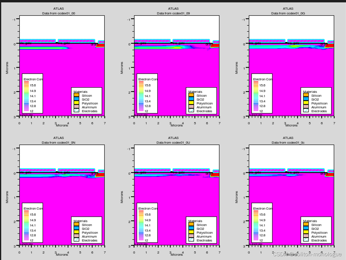
⑧绘制不同状态的图像
# now do transfer
# ramp transfer gate to +2V
log outf=transfer.log
solve v2=2 ramptime=1e-9 dt=1e-11 tstop=1e-6 outf=ccdex01_00 master
tonyplot ccdex01_00 ccdex01_09 ccdex01_0G ccdex01_0N ccdex01_0U ccdex01_0c -set ccdex01_3.set
quit
这个master 还有下边的090G0N什么意思?
字面意思是展示输运过程?

二、唐龙谷书籍中搜索CV特性仿真并进行学习
3.6.2 交流小信号特性
交流仿真的语法和直流仿真的语法很相似,只是添加了频率相关的参数。有两种交流仿真类型,一是频率不变只变直流偏置,一是变频率直流偏置不变。
例:
solve vgate=-5 vstep=0.1 vfinal=5.0 name=gate ac freq=1e6
交流仿真可以得到器件的CV特性,应用在MOS器件仿真则可以得到栅——源电容,栅——漏电容和栅——衬底电容。对于MOS中源和衬底不相接和相连接(由器件编辑器将源和衬底用金属层连接起来)的两种接法下使用下例仿真其交流特性,得到下图所示的电容电压特性

例:交流仿真,变交流频率(能得到两端口的电容随频率变化的特性)。频率从1GHz增加到11GHz,以1GHz为步长。
solve vbase=0.7 ac freq=1e9 fstep=1e9 nfstep=10
例:交流仿真,在初始频率的基础上按倍数增加,从1MHz开始,频率每一次增加为原来的两倍,总共增加10次,这样最后为2^10*1MHz=1.024GHz
solve vbase=0.7 ac freq=1e6 fstep=2 mult.f nfstep=10
例:直流偏置和交流频率一起改变,这会在每一个直流偏置点都对频率进行扫描。
solve vgate=0 vstep=0.05 vfinal=1 name=gate ac freq=1e6 fstep=2 mult.f nfsteps=10
三、唐龙谷书籍中搜索瞬态特性仿真并进行学习
瞬态仿真用于时间相关的测试或响应。瞬态仿真可以由逐段线性方式,指数函数方式和正弦函数方式获得。
例:在ramptime时间内栅压加到1V,然后保持直到tstop,
solve vgate=1.0 ramptime=1e-9 tstep=0.1e-9 tstop=1e-8
示意图:

例:光电器件瞬态响应,光强在ramptime内从5W/cm2减小为0
go atlas
init infile=CCD.str
model srh optr fldmob evsatmod=1 ecritn=6.e3 fermidirac print bgn impact
impact selb an2=1e7 ap2=9.36e6 bn2=3.45e6 bp2=2.78e6
output con.band val.band band.para flowline
method gummel newton trap
beam num=1 x.orgin=0 y.orign=4.0 angle=270.0 wavelength=.8\
back.refl front.refl reflect=5 min.power=0.001
solve b1=5
log outf=photo_current_transient.log master
solve b1=0 ramp.lit ramptime=1e-9 tstop=10e-9 tstep=1e-12
tonyplot photo_current_transient.log -set photo.set
quit


Agent 垂直技术社区,欢迎活跃、内容共建,欢迎商务合作。wx: diudiu5555
更多推荐

 11
11 0
0- 0


 已为社区贡献1条内容

所有评论(0)