
【数电实验5】Verilog—可控分频器设计 & ModelSim的使用
【2022.04西南交大数电实验】5-可控分频器设计 & ModelSim的使用
【2022.04西南交大数电实验】
【本代码及波形已通过老师验收。仅供参考。】
【参考博客:【swjtu】数字电路实验4-可控分频器设计_码龄零年_921的博客-CSDN博客_可控分频器设计】
【2022.05.06更新:若出现Can't generate test bench files -- select a valid simulation tool,则通过菜单栏Assignments—Settings弹出窗口中EDA Tool Settings—Simulation设置为ModelSim,重新编译即可解决: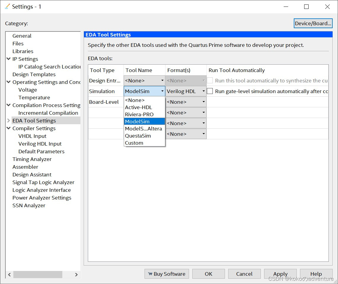
】
目录
1 Quartus代码编写
clk_in 分频器时钟输入;
sel 选择开关;
clk_out 分频器信号输出;
rst_n 清零信号
module yck_1716_5_1(clk_in, sel, clk_out, rst_n);

    input clk_in;
	input sel;
	input rst_n;
	output reg clk_out;

	reg [15: 0]count;

	parameter num1 = 50000000 / 11716;		// 11716为学号后五位 (1/11716)/(1/50000000) 求得与多少个时钟周期相当
	parameter num2 = 50000000 / 1716;		// 1716为学号后四位 (1/1716)/(1/50000000)

	always@(posedge clk_in or negedge rst_n)
	begin

		if(!rst_n)
		begin
			count <= 16'd0;
			clk_out <= 1'b0;
		end

		else if((count < num1 / 4 & sel)	| (count < num2 / 4 & !sel))	//clk_out的占空比D=25%,即1/4
			begin
				count <= count + 16'd1;
				clk_out <= 1'b1;            //赋为高电平
			end

			else if((count < num1 - 1 & sel) | (count < num2 - 1 & !sel))
			begin
				count <= count + 16'd1;
				clk_out <= 1'b0;            //赋为低电平
			end

			else
				count <= 16'd0;
	end

endmoduleparameter的用法:Verilog中的parameter_qq_16923717的博客-CSDN博客_parameter verilog
2 test代码生成
对 yck_1716_5_1.v 进行 Start Compilation ![]() ,而后自动生成test bench代码(如果没有Start Compilation 直接生成test bench代码会报错的):
,而后自动生成test bench代码(如果没有Start Compilation 直接生成test bench代码会报错的): 
在下栏中找到所生成vt文件的路径:


将vt文件中四个位置的代码进行修改如下:
timescale:
`timescale 10 ns/ 1 ns删去:
reg eachvec;初始化代码:
initial
begin
// code that executes only once
// insert code here --> begin
rst_n = 1'b0;
sel = 1'b0;
clk_in = 1'b0;
#100
rst_n = 1'b1;
#300000
sel = 1'b1;
// --> end
$display("Running testbench");
end
always:
always
// optional sensitivity list
// @(event1 or event2 or .... eventn)
begin
// code executes for every event on sensitivity list
// insert code here --> begin
#1
clk_in = ~clk_in;
// --> end
end
新建一个v文件,将修改后的所有代码复制,粘贴到该文件中,而后编译保存。


// Copyright (C) 2018  Intel Corporation. All rights reserved.
// Your use of Intel Corporation's design tools, logic functions
// and other software and tools, and its AMPP partner logic
// functions, and any output files from any of the foregoing
// (including device programming or simulation files), and any
// associated documentation or information are expressly subject
// to the terms and conditions of the Intel Program License
// Subscription Agreement, the Intel Quartus Prime License Agreement,
// the Intel FPGA IP License Agreement, or other applicable license
// agreement, including, without limitation, that your use is for
// the sole purpose of programming logic devices manufactured by
// Intel and sold by Intel or its authorized distributors.  Please
// refer to the applicable agreement for further details.

// *****************************************************************************
// This file contains a Verilog test bench template that is freely editable to
// suit user's needs .Comments are provided in each section to help the user
// fill out necessary details.
// *****************************************************************************
// Generated on "04/24/2022 00:14:15"

// Verilog Test Bench template for design : yck_1716_5_1
//
// Simulation tool : ModelSim (Verilog)
//

`timescale 10 ns/ 1 ns
module yck_1716_5_1_vlg_tst();
// constants
// general purpose registers

// test vector input registers
reg clk_in;
reg rst_n;
reg sel;
// wires
wire clk_out;

// assign statements (if any)
yck_1716_5_1 i1 (
// port map - connection between master ports and signals/registers
	.clk_in(clk_in),
	.clk_out(clk_out),
	.rst_n(rst_n),
	.sel(sel)
);
initial
begin
// code that executes only once
// insert code here --> begin
rst_n = 1'b0;
sel = 1'b0;
clk_in = 1'b0;
#100
rst_n = 1'b1;
#300000
sel = 1'b1;
// --> end
$display("Running testbench");
end
always
// optional sensitivity list
// @(event1 or event2 or .... eventn)
begin
// code executes for every event on sensitivity list
// insert code here --> begin
#1
clk_in = ~clk_in;
// --> end
end
endmodule
代码解读:
① `timescale 时间尺度 / 时间精度
写在所有仿真文件(.v)的代码首行,时间尺度、精度单位定义,时间尺度预编译指令,用来定义模块仿真时的时间单位和时间精度。
注意:仿真时间单位和时间精度的数字只能是1、10、100,不能为其它的数字。而且,时间精度不能比时间单位还要大。最多两者一样大。
【转自`timescale 1ns/1ns 解读_三个刺客的博客-CSDN博客_1ns】
② # + 数字
# 是延迟的意思,# 号后面数字是延迟的数量,延迟的单位由`timescale控制。
比如有:`timescale 1ns/1ps 意思就是时间单位为1ns,精度是1ps 那么,#10.5 就是延迟10.5ns的意思。
注意:在同步时序数字逻辑电路的verilog代码中,不能加入“#”进行延迟,这不是代码编写阶段能决定的。
【转自在verilog中#的用法_Tiger-Li的博客-CSDN博客_verilog中#】
③ 关于被删去的 @eachvec
当测试文件中有时钟信号,并且有@eachvec时,仿真时间很短,如果在它之前有在always过程块里规定时钟信号的翻转的话,这个时钟信号也不会翻转,那一行注释删掉的话仿真才能得到一段很长的波形。
但是当测试文件中没有时钟信号,去掉这一行,仿真就没有波形。推断eachvec是类似时钟信号一样的驱动信号。
在没有clk的程序中,保留eachvec;有clk的程序中,屏蔽eachvec。
【转自【FPGA】TestBench中关于@eachvec_xiao_-_zhu的博客-CSDN博客】
3 ModelSim仿真
打开ModelSim,创建ModelSim工程:


编译: 
配置仿真:


添加波形,设置仿真时长:


运行仿真:

可通过绿色加号添加标尺:

显示设置:


最终效果:
1716Hz,周期为 1 / 1716 ≈ 5.8275 * 10^(-4) s,图上为 582740 ns:

145680 ns : 437060 ns ≈ 1 : 3
11716Hz,周期为 1 / 11716 ≈ 8.535 * 10^(-5) s,图上为 85340 ns:

21320 ns : 64020 ns ≈ 1 : 3

50MHz,周期为 1 / 50000000 = 2 * 10^(-8) s,图上为 20 ns:

4 原始数据记录
| Top-level Entity name | Family | Device |
| yck_1716_5_1 | Cyclone IV E | EP4CE6E22C8 |
| Total logic elements | Total registers | Total pins |
| 36 / 6,272 ( < 1 % ) | 17 | 4 / 92 ( 4 % ) |
| Total memory bits | Embedded Multiplier 9-bit elements | Total PLLs |
| 0 / 276,480 ( 0 % ) | 0 / 30 ( 0 % ) | 0 / 2 ( 0 % ) |
| 信号名 | 主板器件 | PIN |
| clk_in | 50MHz | PIN_90 |
| clk_out | IO0 | PIN_46 |
| rst_n | Key1/SW1 | PIN_31 |
| sel | Key0/SW0 | PIN_24 |
Frq0 = 1716.06Hz,Duty0 = 25.00% :

Frq0 = 11718Hz,Duty0 = 24.98% :


旨在为数千万中国开发者提供一个无缝且高效的云端环境,以支持学习、使用和贡献开源项目。
更多推荐


 127
127 0
0- 0


 已为社区贡献1条内容

所有评论(0)